26 Jun. 2020
The scaling of transistor technology was made possible by controlling the conductivity of semiconductors through the application of an electric field across an insulating gate dielectric. This fundamental principle has remained largely unchanged since 1980s. Note however that despite considerable advances in scaling the size of transistors, voltage and frequency scaling have slowed. Efforts to decrease operating voltages have been hampered by the ‘Boltzmann tyranny’ pertaining to current control (limit of ln(10) kT/q or 60 mV/dec of current at room temperature). This has prompted considerable research effort to develop beyond-CMOS devices. However, researchers have yet to devise a technologically suitable computational logic device with high energy efficiency, high logic density (i.e., computing functions per unit area), non-volatility (to counteract current leakage) and efficient interconnects.
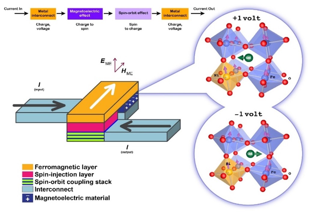
In 2019, the magnetoelectric spin–orbit (MESO) device was proposed. It comprises two technologically scalable transduction mechanisms: ferroelectric/magnetoelectric switching and topological conversion of spin to charge. The device interfaces with electrical interconnects (i.e., it is charge-/voltage-driven) and produces a charge/voltage output, as shown in the representative figure above. The MESO device comprises a magnetoelectric switching capacitor, a ferromagnet, and a spin-to-charge conversion module. Compared to CMOS technology, the MESO device features superior switching energy, lower switching voltage and higher logic density than CMOS. Furthermore, its non-volatility enables the ultralow standby power critical to modern computing.
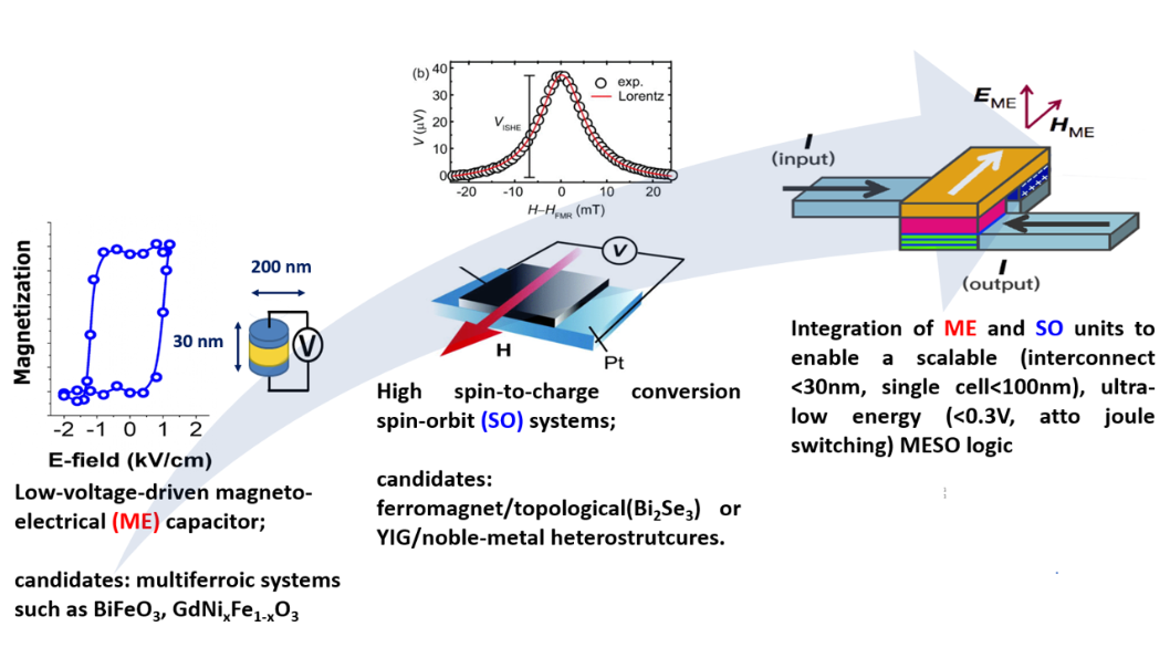
Our research group is committed to developing materials for the continued development of these two transduction mechanisms. Our objective in the current research is to integrate the two material systems (magnetoelectric and SOC) to create a scalable beyond-CMOS spintronic logic device featuring non-volatility and energy-efficient charge-based interconnects. We expect that this device will allow (i) continued scaling in energy per operation toward atto-joule-level switching energy, (ii) substantial improvements in logic density, and (iii) improved scalability for interconnects due to reduced susceptibility to the effects of resistivity. Note that it will also be necessary to devise a path capable of seamlessly integrating the new device with existing CMOS technology.
We believe that the non-volatility and ultra-low energy operations of MESO logic devices will open the door to entirely new computing architectures capable of avoiding the trade-offs inherent in the Turing and von Neumann architectures and Amdahl’s law. New quantum materials, novel integration systems, and alternative logic architectures will usher in a next era of computing beyond advanced CMOS technology.
click here to follow our new publication