NCTU
Function Material Group
Function Material Group
With the progress in silicon circuit miniaturization, lowering power consumption becomes the major objective. Recent developments in the creation of effective negative capacitance in ferroelectrics have further offered a solution in nano-electronics scaling such as reducing supply voltage, heat generation and leakage current, as wellie their potential application in low-power electronics, energy storage, and conversion.
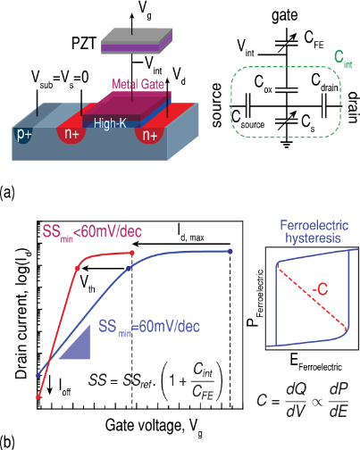
Fig. 1. The investigated experimental configuration of the NCFET (left) and the capacitance model of the structure (right). (a). Transfer characteristics of a non-hysteretic NCFET versus the base MOSFET highlighting the gain of using the ferroelectric negative capacitance in terms of SS improvement and threshold voltage reduction (b). Figure is cited from A. Saeidi et al., 2017 47th European Solid-State Device Research (ESSDERC), European Conference.
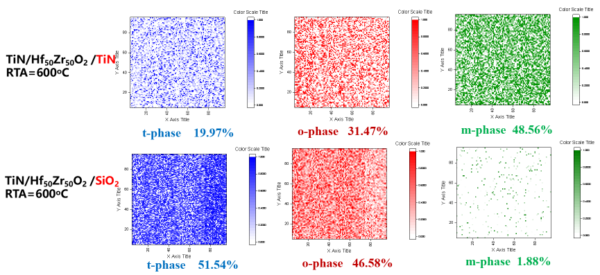
Fig. 2: phase distribution (tetragonal (t), orthorhombic (o) and monoclinic (m) phase) mapped by nano x-ray beam on HZO, which takes advantage of x-ray’s element-specificity-key to solving the phase inhomogeneityissue of NCFET. HZO films were deposited on TiN and SiO2 substrates for comparison.
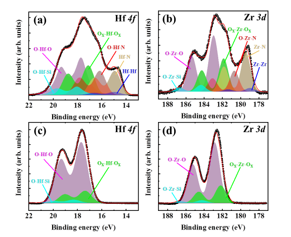
Fig. 3: Core level photoelectron spectra of Hf 4f and Zr 3d recorded for TiN/HZO ((a) and (b)) and TiN/HZO-ref ((c) and (d)). The curve indicated with black symbols (experimental data) overlaps the sum curve of the spectrum (sum) and a Shirley background (BG) used in fitting XPS spectra.
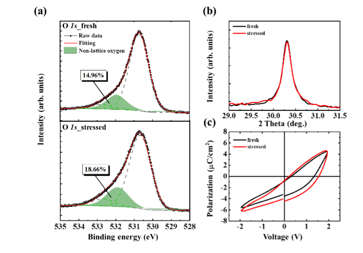
Fig. 4: (a) Core level photoelectron spectra of O 1s for the TiN/HZO, fresh (upper figure) and after-stress-1000s (lower figure) ; fitting heighted by green color indicates the contribution from the non-lattice oxygen (i.e., oxygen vacancy, Ox); (b) O-phase (111o) characteristic diffraction peaks and (c) P-E hysteresis loops recorded for TiN/HZO fresh (black) and post-stress-1000s (red).
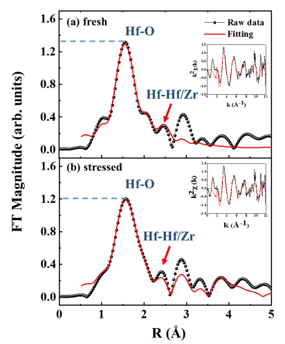
Fig. 5: The Hf L3-edge FT-EXAFS spectra (black) and their respective fitting results (red) for the TiN/HZO with (a) fresh and (b) stressed conditions. Horizontal dashed lines identify the difference in FT-EXAFS magnitude between the two samples which is associated with the level of atomic ordering around Hf. Insets show the Chi vs k spectra.
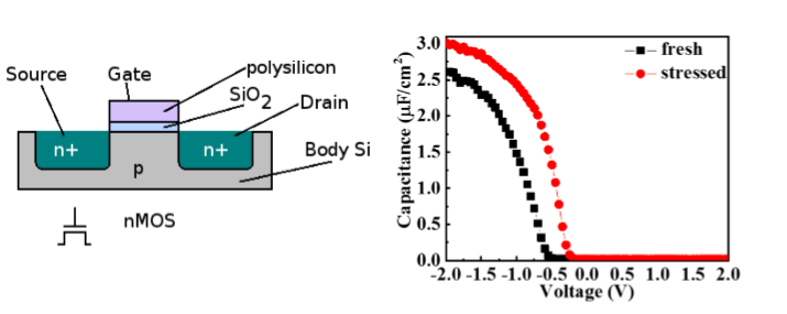
Fig. 6: (left) schematic of a MOS capacitor structure; (right) capacitance-voltage (C-V) performance of the TiN/HZO with fresh (black) and stressed (red) conditions.
click here to follow our new publication