08 Jul. 2019
We aim to develop new compounds or novel hybrid structures which possess potential to be operated with low-energy consumption. For example, multiferroic devices are potentially suitable for application of electrical (voltage) controlled devices, owing to the coexistence of ferroelectric (FE) and magnetic orders in a single phase. Therefore, the idea of making spintronic devices based on multiferroic materials comes very naturally. We synthesized a new multiferroic GdFe0.8Ni0.2O3 (GFNO) thin film that features coupled FE and antiferromagnetic (AFM) orders at room temperature. The FE and magnetic orders of the film are very responsive to low applied voltages (+/- 1 volt) and the multiferroic behavior is sensitive to bias polarity. Thus, this material could double the number of available magnetic read-out states within a low voltage regime, which satisfies the requirements for low-power and high-storage technology.
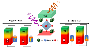
Fig. 1: Illustration showing control over multiple magnetic states (relying on Co/GFNO interface magnetic coupling) via cross-tuning of bias and polarity.
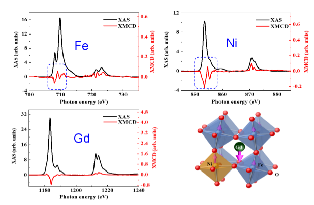
We utilized x-ray magnetic circular dichroism (XMCD) to probe atomic moment of the GFNO. Since XMCD is element-specific, we were able to discriminate the atomic moments of Gd, Ni and Fe. Surprisingly, we found that Ni possesses an atomic moment ~ 5 times larger than that of Fe. This means that Ni likely has a much stronger magnetic interacions with Gd than Fe.
Fig. 2: XAS/XMCD spectra for GFNO film: (a) Fe L2, 3-edges, (b) Ni L2, 3-edges, and (c) Gd M4, 5-edges (XAS and XMCD intensities read from left (black) and right (red) y-axes, respectively). Spectra were collected using the partial fluorescence yield (PFY) method. XMCD spectra were normalized to corresponding XAS spectral-jump for a quantitative comparison. (d) spin-configuration in relation to crystallographic nature of GFNO.
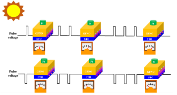
Secondly, if deposited on SrTiO3 (STO) perovskite substrate, we found that the GFNO can function as pulse-controlled non-volatile memory devices without the need for an electrical-stressing read-out process. Under an applied pulse voltage, the GFNO/STO devices exhibited superior energy storage performance, in which short circuit current (Jsc) is controlled by altering the direction and number of applied pulses. Modulating the duration and direction of continuous pulse voltage is an effective method for controlling Jsc, thereby allowing the fabrication of non-destructive, light-tunable, non-volatile memory devices. The proposed device differs fundamentally from other memory devices that require external voltage for read operations, which often leads to erasure of written signals.
Fig. 3: Pulse-driven non-volatile perovskite memory with photovoltaic read-out characteristics.
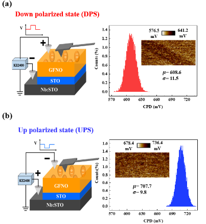
For the GFNO/STO device, the application of a negative pulse-wave generated an upward-polarization-state (UPS). The band bending generated by opposing polarizations at the surface of the GFNO were visualized using kelvin piezoelectric force microscope (KPFM) measurements to probe local surface potential. The two states differ in local surface potential, which depends on the relative polarization charges and screening charges.
Fig. 4: (a) (left) Illustration of pulse poling (DPS and UPS) in Pt/GFNO/STO/Nb:STO devices and resulting polarization alignment within GFNO layer: (right) KPFM-derived CPD distributions where µ and σ respectively represent mean and standard deviation of distribution associated with (a) DPS and (b) UPS; (insets) surface potential maps.
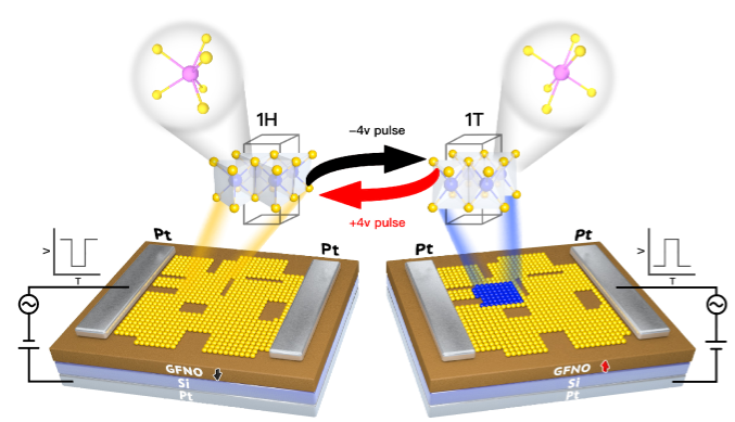
We also fabricated pulse-controlled MoS2 phase transition on the perovskite ferroelectric GFNO layer. We demonstrate the tuning of electrical characteristics using pulse voltage to evoke a 1H-1T phase transition in the single-layer MoS2. Locally reversing the ferroelectric polarization of the GFNO through the application of pulse voltage makes it possible to manipulate the carrier concentration and associated phase of the single-layer MoS2 via heterostructure interactions. These many features make the proposed device able to function as a pulse-controlled FeFET. The design established in this study paves the way to the development of laterally 2D FeFET, which could provide non-volatile characteristics with a less-destructive read-write process.
Fig. 5: Summary figure depicting pulse-tunable electronic phase of MoS2 channel in an field effect transistor (FET) framework.
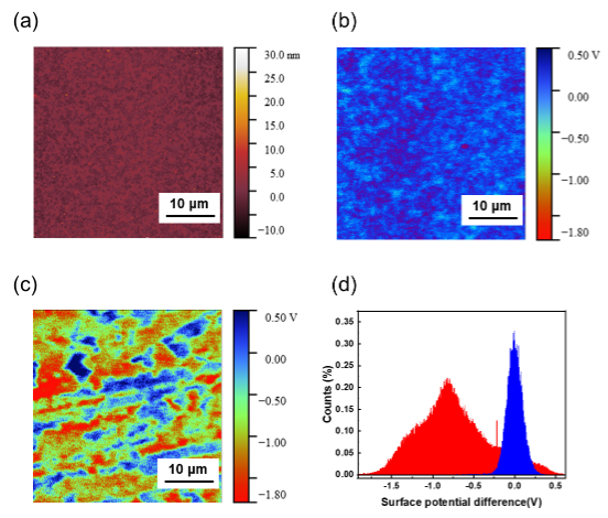
In MoS2/GFNO device, we found that locally reversing the ferroelectric polarization of the perovskite GFNO through the application of pulse voltage makes it possible to manipulate the carrier concentration and associated phase of the MoS2 via heterostructure interactions. We used several imaging tools to characterize the pulse-induced phase transition.
Figure 6: (a) Topographic image of the MoS2/GFNO device without an applied pulse voltage. (b) Surface-potential maps obtained using KPFM under the application of a positive pulse (+4 volts) and (c) negative (-4 volts) pulse. (d) Histogram of surface potential maps indicating variations in CPD in the MoS2/GFNO device under negative and positive pulse states.
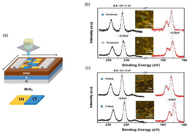
Analysis of the non-volatile properties of the FeFET using the scanning photoelectron spectroscopy revealed that the transition indeed occurred across much of the device landscape.
Figure 7: (a) illustration of methods used to obtain scanning XPS measurements from MoS2/GFNO device; (b) Mo 3d (black) and S 2p (red) core-level photoelectron spectra measured using scanning XPS in various regions of the MoS2 surface under 900 pulse cycles at -4 volts. (c) Mo and S spectra of MoS2 collected from the 1H (upper) and 1T (lower) zones resulting from 900 pulse cycles at -4 volts.
click here to follow our new publication