08 Jul. 2019
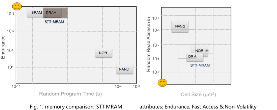
Rapid development in the internet of things, big data, and cloud computing are driving demand for quick, scalable, non-volatile storage devices with low power consumption. Magneto-resistive random access memory (MRAM) features the non-volatile characteristics of flash memory, with access speeds approaching those of SRAM, as well as capacity, density, and service life matching those of DRAM with far lower average power consumption. MRAM appears poised to become a universal memory solution in the near future.
A magnetic tunnel junction (MTJ) consists of two layers of magnetic metal, such as cobalt-iron, separated by an ultrathin layer of insulator, typically aluminum oxide with a thickness of about 1 nm. MTJ is the core of MRAM technology. In MTJ, the insulating layer is so thin that electrons can tunnel through the barrier if a bias voltage is applied between the two metal electrodes. In MTJs the tunneling current depends on the relative orientation of magnetizations of the two ferromagnetic layers, which can be changed by an applied magnetic field. This phenomenon is called tunneling magnetoresistance (TMR) which is a consequence of spin-dependent tunneling.
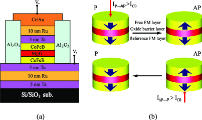
Fig. 2: (a) Structure of magnetic tunnel junction (MTJ) mainly composed of three thin layers: two ferromagnetic layers and one oxide barrier (CoFeB/MgO/CoFeB). (b) Spin transfer torque switching mechanism: the MTJ state changes either from parallel (P) to antiparallel (AP) if the electrons flow from top (I P → A P > I C 0 ), or from AP to P as the electrons are injected from the bottom (I A P −> P > I C 0 ). Data Figure cited from E. Deng et al., IEEE Transactions on Nanotechnology 14, 169 (2015).
We conducted interface analysis on MTJ using high resolution TEM and x-ray photoelectron spectroscopy (XPS). We investigated interface properties of single- and dual-MgO MTJ samples. The dual-MgO structure appeared to favor boron (B) diffusion but prevent capping-layer (Ta) penetration across the interface. This suppressed the dead-layer effect and promoted overall magnetization despite PMA (perpendicular magnetic anisotropy) degradation.
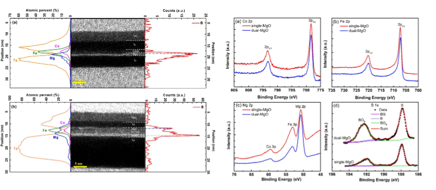
Fig. 3: (left) cross-section TEM images of (a) single-MgO (b) dual-MgO, with corresponding EDX (left) and EELS (right) scanning profiles across the interface. EELS shows only the B distributions. (right) Core level XPS spectra of (a) Co 2p (b) Fe 2p (c) Mg 2p and (d) B 1s recorded from single-MgO and dual-MgO. In (d), the curve indicated by black squares (experimental data) matches perfectly with the sum curve, in which a Shirley background is applied to XPS spectral-fitting.
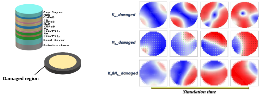
Our group focuses on MRAM failure analysis (soft and hard errors) for MRAM, based on MRAM reliability, spin transfer characteristics, and the key mechanisms for performance degradation. We are establishing independent MRAM failure analysis models aimed at improving reliability, optimizing MRAM components, and increasing yield. For example we perform micromagnetic simulation for magnetic tunnel junction (MTJ)’s switching properties with various damaged conditions, as assigning damaged anisotropy constant (Ku), saturation magnetization (Ms) caused by side-wall damage. This helps to predict MRAM’s performance caused by the etching process.
Fig. 4: illustration showing MTJ stacking (left, upper), where the damaged region (left, bottom) is defined as a black rim area. On the right hand side showing simulated magnetic switching domain behaviors under situations of Ku- (upper), Ms-(middle), and both Ku/Ms-(bottom) conditions.
We simulate magnetization loops of MTJs considering step MTJ stacking with various Ku & Ms damage combinations. This is key to optimization of MTJ fabrication parameters that influence reliability.
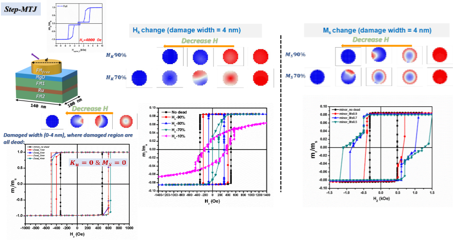
Fig. 5: Construction of theoretical models for side-wall damage to predict MTJ’s magnetic properties with various Ku & Ms damage combinations.
We try to develop MTJ structure-based reliability models of MRAM failures caused by MTJ hard errors, followed by analysis of MRAM failure mechanisms in conjunction with various detection techniques. The ultimate aim is to correct reliability problems; in the following we show that by obtaining R-H loops measured at various voltages, we are able to construct a switching phase diagram (SPD) which provides critical information about backhopping, spin-transfer-torque, voltage-controlled magnetic anisotropy, self-heating, etc.
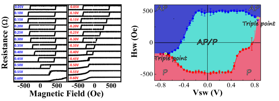
Fig. 6: R-H loops measured at various applied voltages (left). Switching phase diagram (SPD, right side) is constructed by plotting Hswitching and Vswitching.
Since knowing that failure such as dielectric breakdown occurs at interface, we prepared MTJs with different Mg insertions (four types) as shown below, and fabricated them into different sizes (30, 80, 130 and 180 nm), and characterize their electrical transport properties in order to know how interface properties affect the breakdown as MTJ shrinks.
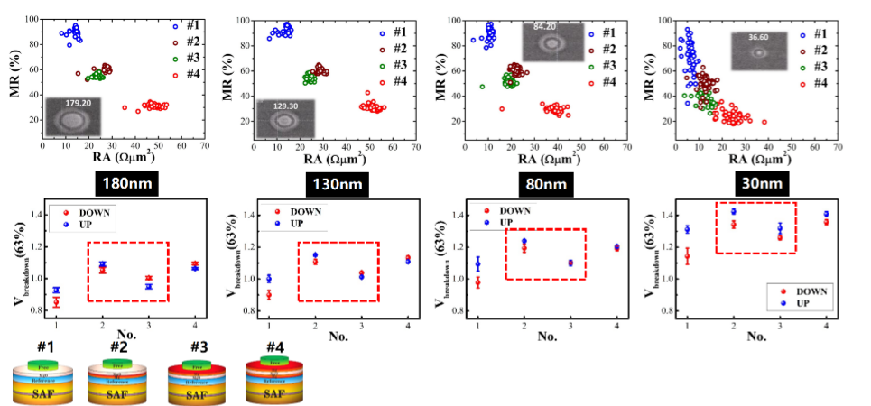
Fig. 7: magneto-resistance (MR) ratio, resistance-area (RA) product and breakdown voltage for four MTJ types featuring different Mg-insertions (layer with red color) and sizes (30, 80, 130 and 180 nm).
click here to follow our new publication